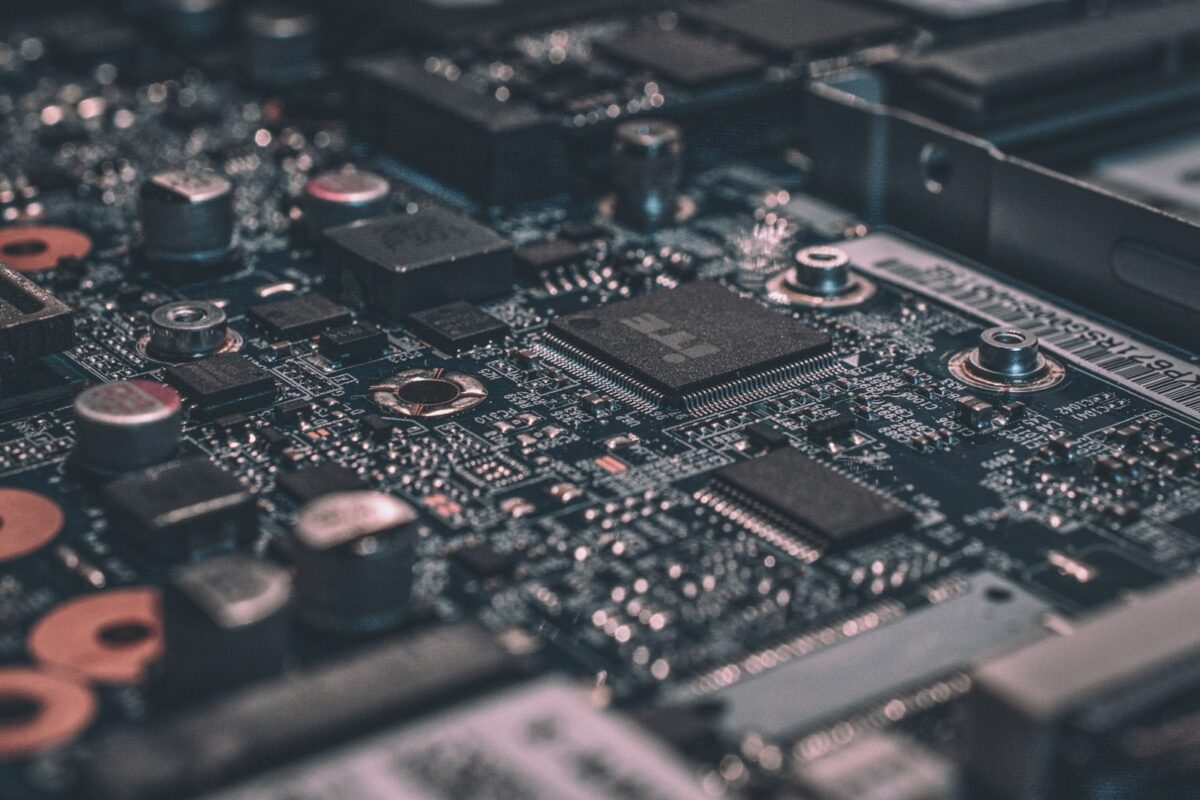
The insatiable appetite of frontier artificial intelligence has officially collided with the thermodynamic realities of modern semiconductors. As state-of-the-art foundation models exceed hundreds of billions of parameters, classical CMOS electronic architectures face an escalating crisis: the Von Neumann memory bottleneck and catastrophic thermal dissipation limits. In modern GPU clusters, more than 60% of total operational energy is consumed not by mathematical computation, but by shuttling electrical charges across metal interconnects between memory banks and arithmetic logic units (ALUs).
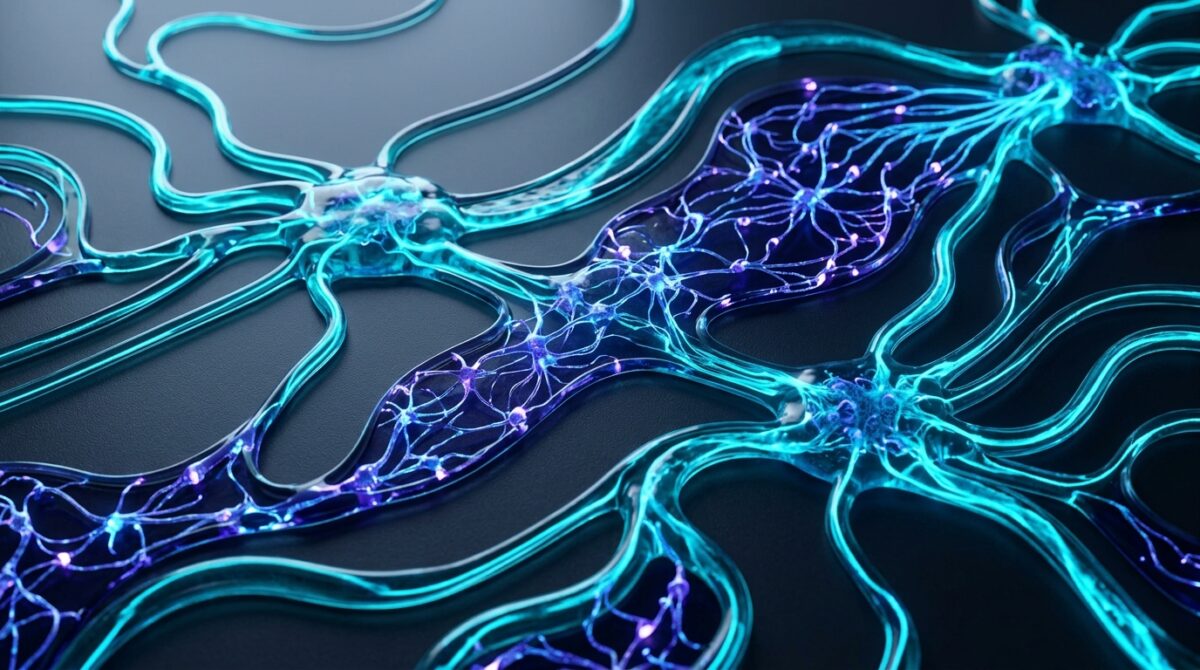
To circumvent the approaching ceiling of Moore’s Law and Dennard scaling, computer architects are turning toward radical non-Von Neumann paradigms. Leading this physical revolution are two complementary architectures: Photonic Integrated Circuits (PICs) that execute tensor operations at the speed of light, and Neuromorphic Computing systems that emulate the event-driven, analog dynamics of biological neural synapses.
The Thermodynamic Wall in Electronic Silicon
Modern semiconductor scaling down to 3nm and 2nm nodes has brought quantum mechanical tunneling, leakage currents, and RC interconnect delays to the forefront of hardware engineering. In dense deep neural networks, matrix-vector multiplication (GEMM) dominates compute workloads. Executing a 16-bit floating-point multiply-accumulate (MAC) operation electronically costs approximately 1 to 3 picojoules (pJ), but moving those operands across an off-package memory bus incurs 100 to 200 pJ.
As clusters scale to tens of thousands of GPUs (e.g., GB200 and H100 pods), interconnect networks require immense electrical power. Optical co-packaged optics (CPO) and on-chip optical tensor processing eliminate these copper trace penalties by utilizing photons rather than electrons for both inter-chip telemetry and core linear algebra.
Optical Tensor Processing: Linear Algebra at the Speed of Light
Photonic processing units (OPUs) utilize Mach-Zehnder Interferometers (MZIs) and silicon micro-ring resonators configured in mesh topologies. In an optical tensor core, weight matrices are encoded into physical phase shifts within light-guiding silicon waveguides. As coherent laser beams propagate through the interferometer grid, interference patterns physically compute matrix multiplications in the analog domain with propagation latencies measured in picoseconds.
| Architectural Metric | Leading Electronic Tensor Core (H100/B200) | Optical Photonic Processor (MZI Mesh) | Neuromorphic Architecture (SNN/Spiking) |
|---|---|---|---|
| Primary Information Carrier | Electrons (Voltage / Charge) | Photons (Phase / Wavelength) | Sparse Action Potentials (Spikes) |
| Energy per MAC Operation | 0.5 – 1.8 pJ | < 0.05 pJ (Passive MZI) | < 0.01 pJ (Event-Driven) |
| Latency per Layer (GEMM) | Nanoseconds (Clock Cycles) | Sub-picosecond (Propagation) | Asynchronous / Dynamic |
| Memory Architecture | Von Neumann (HBM3e / SRAM) | Weight-in-Interferometer (Analog) | Collocated In-Memory Processing |
| Best-Suited Workloads | Training & High-Precision Inference | Dense Matrix Inference & Attention | Continuous Sensory & Edge Robotics |
Wavelength Division Multiplexing (WDM) for Massive Parallelism
One of the most profound advantages of optical computing is Wavelength Division Multiplexing (WDM). In a single physical optical waveguide, dozens of distinct laser frequencies (colors) can travel simultaneously without electromagnetic crosstalk or destructive interference. Each individual wavelength can modulate an independent vector element, enabling a single silicon waveguide to perform multidimensional tensor convolutions in parallel across a single physical trace.
Neuromorphic Silicon: Event-Driven, Sparse Intelligence
While photonics solves the speed and throughput bottleneck of dense matrix mathematics, neuromorphic computing solves the idle power and temporal perception bottleneck. Biological brains consume approximately 20 watts of power while orchestrating trillions of synaptic connections. They achieve this biological efficiency through two core mechanisms: extreme sparsity and asynchronous event-driven communication.
In conventional deep neural networks, every neuron computes its activation at every forward pass, regardless of whether the incoming signal changed. Neuromorphic architectures (such as Intel’s Loihi 2, SynSense, and IBM TrueNorth) replace dense matrix multiplications with Spiking Neural Networks (SNNs). Silicon neurons only transmit binary spikes when their integrated membrane voltage crosses an activation threshold.
The Engineering Challenges: Co-Packaging, Calibration, and ADC/DAC Overhead
Despite their theoretical superiority, photonic and neuromorphic processors face significant engineering hurdles before replacing conventional server racks:
- Analog-to-Digital Conversion (ADC/DAC) Overhead: Optical tensor processors calculate analog phase products, but digital host systems require floating-point numbers. Converting high-bandwidth signals between analog light and digital bits consumes significant power, necessitating end-to-end optical interconnects.
- Thermal Drift and Optical Phase Calibration: Silicon waveguides expand and contract with microscopic temperature variations, altering the refractive index of Mach-Zehnder arms. Advanced micro-heaters and closed-loop phase-calibration circuits are mandatory to maintain numerical precision.
- Software Compilers and Non-Differentiable Operators: Classical deep learning frameworks (PyTorch, JAX) rely on automatic differentiation (Autograd) designed for IEEE 754 floating-point math. Compiling transformer attention mechanisms into spiking event networks or analog interferometer arrays requires entirely new intermediate representations (IRs).
The Hybrid Era: Silicon Co-Packaging and Heterogeneous SoCs
The immediate future of AI infrastructure is not a complete displacement of silicon GPUs, but rather a heterogeneous co-packaged convergence. We are already observing the first commercial manifestations of optical I/O chiplets directly integrated on 2.5D substrate interposers alongside high-bandwidth memory (HBM3e) and digital compute dies.
As foundational models continue their expansion toward AGI, the marriage of optical matrix acceleration for dense transformer layers and neuromorphic event-driven processors for continuous sensory streams represents humanity’s clearest path toward sustainable, superintelligent computing systems.