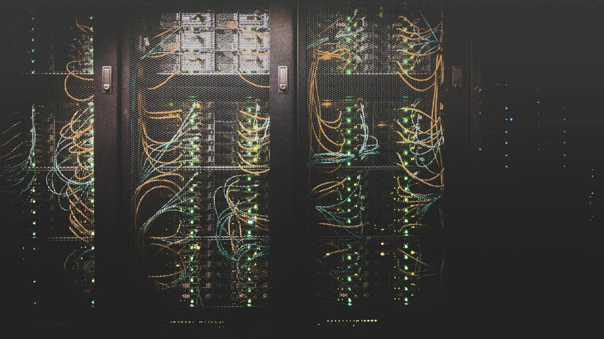
The exponential scaling of frontier foundation models and test-time reasoning compute has triggered an unprecedented arms race in datacenter silicon. Hyperscale cloud providers face a critical strategic crossroads: continue investing billions of dollars in commercial merchant silicon dominated by NVIDIA’s Blackwell architecture, or accelerate internal custom ASIC programs such as Google’s TPU v5p/v6e, Amazon’s Trainium2/Inferentia2, and Microsoft’s Maia 100. This in-depth engineering analysis breaks down the microarchitectural trade-offs, interconnect topologies, software ecosystem lock-in, and total cost of ownership (TCO) shaping modern AI infrastructure.
The Datacenter Scaling Bottleneck: Power, Thermal, and Memory Walls
Modern frontier training clusters spanning 100,000+ accelerators no longer hit compute-bound limits; they collide with physical infrastructure walls:
- The Memory Wall: While raw FP8/FP4 tensor compute has scaled by over $1000\times$ in the past decade, high-bandwidth memory (HBM) capacity and memory bus bandwidth have scaled far more conservatively, creating severe memory-bound stalls during autoregressive token generation.
- The Thermal and Power Wall: Modern accelerator nodes draw between $1,200 \text{ W}$ and $2,700 \text{ W}$ per socket. Datacenters have surpassed air-cooling heat dissipation thresholds, mandating universal transition to direct-to-chip liquid cooling infrastructure.
- The Interconnect Fabric Bottleneck: Large models require distributing weights and activations across thousands of chips via all-to-all collective operations. Network latency and bisection bandwidth dictate cluster scaling efficiency.

Microarchitectural Breakdown: Blackwell B200 vs Custom Cloud ASICs
Evaluating datacenter silicon requires comparing compute density, memory hierarchies, interconnect bandwidth, and software abstraction layers:
| Hardware Architecture | Dense Compute (FP8/FP4) | HBM Capacity & Bandwidth | Interconnect Bandwidth | Cooling Architecture | Software Ecosystem |
|---|---|---|---|---|---|
| NVIDIA B200 (Blackwell) | 4.5 PFLOPS (FP8) / 9.0 PFLOPS (FP4) | 192 GB HBM3e @ 8.0 TB/s | 1.8 TB/s NVLink 5 | Direct Liquid Cooling (DLC) | CUDA, TensorRT-LLM, Megatron |
| Google TPU v5p | 459 TFLOPS (BF16) | 95 GB HBM2e @ 2.76 TB/s | 4.8 Tbps ICI (3D Torus) | Liquid Cooling Circuit | XLA, JAX, PyTorch/XLA |
| AWS Trainium2 | 1.3 PFLOPS (FP8) | 96 GB HBM @ 3.2 TB/s | NeuronLink-v2 (Non-blocking) | Hybrid Liquid/Air | AWS Neuron SDK |
| Microsoft Maia 100 | 1.6 PFLOPS (FP8) | 64 GB HBM2e @ 1.8 TB/s | Custom Ethernet RoCEv2 | Custom Liquid Sidecar | ONNX Runtime, Triton |

Mathematical Foundations: Roofline Model and Interconnect Bisection Scaling
The operational throughput $W$ of a datacenter accelerator is bound by the classic Roofline Model, balancing arithmetic intensity $I$ (FLOPs per byte) against memory bandwidth $\beta$ and peak computational capacity $\Pi$:
$$W = \min(\Pi, \ I \cdot \beta)$$
For distributed model-parallel training across $N$ accelerators, the cluster bisection scaling penalty is dictated by collective all-reduce communication latency:
$$T_{\text{comm}} = \alpha + \frac{2(N-1)}{N} \frac{M}{\text{BW}_{\text{interconnect}}}$$
Where $\alpha$ is network link latency, $M$ is gradient payload size, and $\text{BW}_{\text{interconnect}}$ is bidirectional bus bandwidth. NVIDIA’s $1.8 \text{ TB/s}$ NVLink 5 provides up to $4\times$ higher bisection bandwidth than standard RoCEv2 Ethernet fabrics, maintaining high scaling efficiency on clusters exceeding 32,000 GPUs.
Frequently Asked Questions
Why do cloud hyperscalers invest billions in custom ASICs if NVIDIA is faster?
Hyperscalers develop custom ASICs (like TPU and Trainium) to reduce dependency on NVIDIA’s high profit margins (over 75%), gain control over datacenter rack thermals and power delivery, and offer internal services like search and recommendation at dramatically lower operational cost.
What makes CUDA such an enduring moat for NVIDIA?
CUDA represents two decades of low-level hardware kernel optimization. Hundreds of thousands of open-source repositories, libraries (cuDNN, CUTLASS), and compiler optimizations are written natively for CUDA, requiring extensive engineering effort to port to competing SDKs.
What is the difference between NVLink and standard InfiniBand/Ethernet?
NVLink is a proprietary, ultra-low-latency chip-to-chip interconnect designed for intra-rack GPU communication, functioning essentially as an extended memory bus. InfiniBand and RoCEv2 Ethernet are networking protocols designed for inter-rack and cluster-wide connectivity.
How does liquid cooling impact modern AI datacenter construction?
Modern high-density server racks drawing 100 kW to 120 kW per rack cannot be cooled by ambient air fans alone. Direct-to-chip liquid cooling circulates treated dielectric coolants directly over GPU copper cold plates, cutting facility cooling energy use by over 30%.
References and Academic Citations
- Jouppi, N. P., et al. (2023). “TPU v4: An optically reconfigurable supercomputer for machine learning with hardware support for embeddings.” ACM/IEEE International Symposium on Computer Architecture (ISCA).
- NVIDIA Corporation (2024). “NVIDIA Blackwell Architecture Technical Whitepaper.” NVIDIA Technical Reports.
- Williams, S., Waterman, A., & Patterson, D. (2009). “Roofline: An insightful visual performance model for multicore architectures.” Communications of the ACM, 52(4), 65-76.
- Shoeybi, M., et al. (2019). “Megatron-LM: Training multi-billion parameter language models using model parallelism.” arXiv preprint arXiv:1909.08053.