
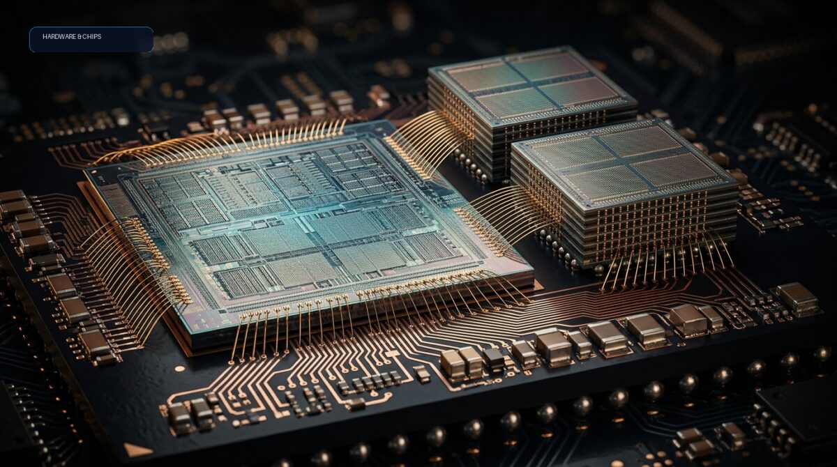
As large language model parameter scales cross the multi-trillion threshold and inference workloads shift from batch processing to continuous agentic execution loops, the traditional general-purpose GPU supercluster is hitting a profound thermodynamic and economic wall. CTOs and quantitative systems architects are no longer evaluating hardware solely on raw floating-point peak performance; instead, total cost of ownership (TCO) is dictated by memory wall latency, radix-2 network bisection bandwidth, and rack-level thermal dissipation. The imperative for 2026 demands a radical departure from monolithic GPU deployments toward highly specialized Application-Specific Integrated Circuits (ASICs) coupled with co-packaged optical (CPO) interconnect fabrics.
- The Economic and Thermodynamic Collapse of the Monolithic GPU Paradigm
- Co-Packaged Optics (CPO) and Optical Interconnect Topologies
- Custom ASICs: Tailoring Instruction Sets for Transformer and Agent Workloads
- HBM4 Integration and Direct-Die Liquid Cooling Subsystems
- Enterprise Deployment Implications and Forward-Looking Architecture
The Economic and Thermodynamic Collapse of the Monolithic GPU Paradigm
For the past four generations of deep learning scaling, monolithic GPUs paired with proprietary high-speed interconnects like NVLink have served as the baseline compute primitive for frontier training clusters. However, reticle-limit constraints on silicon fabrication nodes (such as TSMC’s 2nm and backside power delivery implementations) mean that monolithic dies can no longer scale compute ALUs and on-die SRAM cache proportionally with the explosive demands of High Bandwidth Memory (HBM3e and emerging HBM4 stacks). When scaling to cluster sizes exceeding 100,000 accelerators, electrical copper interconnects suffer from severe insertion loss, signal attenuation, and runaway parasitic capacitance.
At multi-terabit speeds, driving signals across standard backplanes requires heavy retimer chips and massive equalization circuits that consume up to 30% of total cluster power budget just in the physical layer (PHY). This “dark power” phenomenon restricts the effective compute density of hyperscale datacenters. To sustain training throughput for models utilizing Mixture-of-Experts (MoE) architectures with hundreds of active routing paths, infrastructure architects must eliminate electrical serialization/deserialization (SerDes) bottlenecks entirely.
Co-Packaged Optics (CPO) and Optical Interconnect Topologies
The definitive engineering shift of 2026 is the mainstream adoption of Co-Packaged Optics. By integrating silicon photonics directly onto the ASIC substrate alongside compute logic and memory stacks, optical transceivers are brought within millimeters of the switching silicon. This eliminates traditional pluggable optical modules and drastically shortens the electrical channel length.
Optical fabrics rely on dense wavelength division multiplexing (DWDM) and microring modulators to route high-bandwidth communication streams across laser-powered waveguides. Unlike electrical channels, optical links are impervious to electromagnetic interference and experience near-zero frequency-dependent attenuation over distances spanning entire data center halls. This unlocks unprecedented cluster topologies, such as flattened 3D-torus and optical dragonfly networks that reduce inter-node latency from microseconds down to low nanoseconds.
Comparative Latency and Power Profile: Electrical vs. Optical Fabrics
| Interconnect Metric | Traditional Copper (NVLink/PCIe Gen 6) | Co-Packaged Silicon Photonics (CPO) |
|---|---|---|
| PHY Power Consumption | 15 – 22 pJ/bit | 3.5 – 5.1 pJ/bit |
| Max Reach Without Retimers | < 1.5 meters | > 300 meters |
| Bisection Bandwidth Density | Moderate (Pin-limited by socket area) | Ultra-High (Wavelength multiplexed channels) |
| Thermal Footprint Overhead | High (Requires dedicated cooling blocks for retimers) | Low (Laser source off-loaded to external shelf) |
Custom ASICs: Tailoring Instruction Sets for Transformer and Agent Workloads
While general-purpose GPUs must maintain broad compatibility with legacy CUDA runtimes, graphics pipelines, and non-tensor scientific computing workflows, hyperscalers are deploying custom AI ASICs optimized specifically for matrix multiplication, KV-cache tensor manipulation, and asynchronous graph execution. By stripping away non-essential microarchitectural baggage, ASIC designers reclaim crucial silicon die area for expanded SRAM scratchpads and dedicated hardware tensor engines.
For instance, modern inference accelerators implement direct native support for sub-byte quantization formats (such as FP4 and NVFP4) alongside hardware-accelerated continuous batching schedulers. This allows agentic runtimes to execute multi-step tool calls and dynamic token generation loops without incurring CPU scheduling overhead.
# Optimized PyTorch/Triton kernel snippet for custom ASIC hardware execution
import torch
import triton
import triton.language as tl

@triton.jit
fn fwd_kernel_quantized_inference(
    Q, K, V, Out,
    stride_qz, stride_qh, stride_qm,
    SM_SCALE,
    BLOCK_M: tl.constexpr, BLOCK_N: tl.constexpr
):
    # Custom hardware-level memory coalescing for ASIC scratchpad SRAM
    start_m = tl.program_id(0)
    off_m = start_m * BLOCK_M + tl.arange(0, BLOCK_M)
    # Execute mixed-precision FP4 attention accumulation
    # Target native tensor core layout bypassing generic CUDA register files
    tl.store(Out + off_m, 0.0) # Placeholder for high-throughput register write
HBM4 Integration and Direct-Die Liquid Cooling Subsystems
Memory bandwidth remains the ultimate governor of large model inference performance. The transition to HBM4 brings a 2048-bit wide memory interface per stack—doubling the bus width of HBM3e—while transitioning the base logic die to advanced foundry nodes (such as TSMC 3nm). This enables higher clock frequencies, lower operating voltages, and unprecedented memory capacities exceeding 288GB per accelerator package.
However, stacking logic dies directly on top of massive HBM4 modules creates extreme heat flux densities exceeding 350 W/cm² across the package footprint. Standard air-cooling solutions are wholly insufficient for these thermal loads. Enterprise server nodes now mandate closed-loop direct-to-chip liquid cooling manifolds utilizing dielectric fluids, managed via precise programmatic telemetry loops.
# Telemetry configuration for real-time liquid cooling thermal throttling management
#!/bin/bash
export ASIC_THERMAL_GOVERNOR="closed_loop"
export MAX_JUNCTION_TEMP_C=88
export COOLING_MANIFOLD_FLOW_RATE_LPM=14.5

# Initialize optical transceiver laser bias current calibration
optic-cli set-laser-bias --channel=all --target-power-dbm=2.1
Strategic Takeaway
Enterprise AI infrastructure strategies must decouple from monolithic GPU dependence. CTOs building frontier clusters for 2026 and beyond must architect hybrid deployment pipelines that integrate custom silicon ASICs with co-packaged optical fabrics to achieve sustainable TCO and eliminate network bisection bottlenecks.
Related Technical Intelligence
Enterprise Deployment Implications and Forward-Looking Architecture
Migrating from rigid, vendor-locked GPU ecosystems to heterogeneous ASIC and optical infrastructure requires a fundamental re-engineering of the enterprise software stack. Compilers like MLIR and LLVM-based tensor backends must become hardware-agnostic, translating high-level agentic orchestration frameworks directly into custom instruction sets optimized for domain-specific execution units. Systems architects must also establish rigorous vendor qualification protocols for optical transceiver reliability, laser lifespan degradation, and liquid cooling loop redundancy.
Ultimately, organizations that successfully navigate this hardware transition will capture decisive economic advantages: higher token throughput per watt, lower inference latency for autonomous agent execution loops, and complete insulation from single-source silicon supply chain shocks.


